


Odisha Secures First-Ever Semiconductor Project Under India Semiconductor Mission
Union Cabinet clears two high-tech manufacturing units worth ₹4,600 crore in Bhubaneswar
Bhubaneswar: In a landmark development that places Odisha firmly on India’s semiconductor map, the Union Cabinet, chaired by Prime Minister Narendra Modi, on Tuesday approved two advanced semiconductor projects in Bhubaneswar under the India Semiconductor Mission (ISM). The decision marks Odisha’s debut in chip manufacturing and is expected to catalyse the state’s transformation into a key electronics and high-tech manufacturing hub.
Part of National Semiconductor Push
The Odisha-based units are among four semiconductor projects cleared nationwide, with a total investment of ₹4,600 crore. This approval takes the overall tally of ISM-backed projects to 10 across six states, attracting cumulative investments of ₹1.60 lakh crore. The move signals India’s accelerated drive towards self-reliance in semiconductor production—a sector critical to defence, electric mobility, artificial intelligence, and renewable energy.
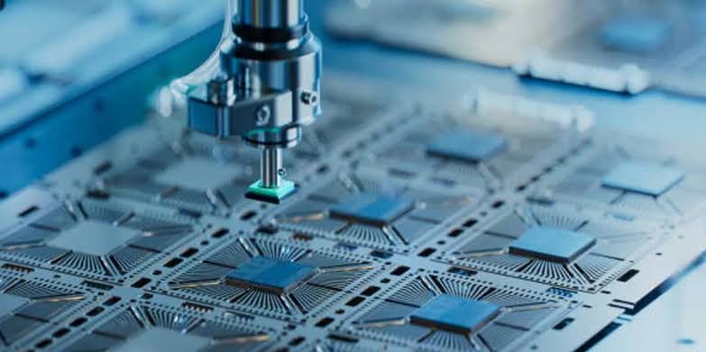
First Silicon Carbide Semiconductor Fabrication in India
One of the two projects will be spearheaded by SiCSem Pvt Ltd in collaboration with UK-based Clas-SiC Wafer Fab Ltd. Set to be located in Info Valley, Bhubaneswar, the facility will be India’s first commercial silicon carbide (SiC) semiconductor fabrication unit. It will boast an annual production capacity of 60,000 wafers and a packaging output of 96 million units.
Silicon carbide chips are renowned for their high efficiency and performance in extreme conditions, making them vital for defence equipment, electric vehicles, solar power systems, and railway electrification. By entering this niche manufacturing segment, Odisha is positioning itself as a strategic player in the global compound semiconductor supply chain.
3D Glass Solutions Unit for Advanced Packaging
The second project will be developed by 3D Glass Solutions Inc., focusing on advanced packaging and embedded glass substrate manufacturing. This facility will annually produce 69,600 glass panel substrates, 50 million assembled units, and 13,200 three-dimensional heterogeneous integration (3DHI) modules.
Using advanced technologies such as glass interposers, silicon bridges, and 3DHI modules, the plant will cater to applications in AI-driven systems, high-performance computing, defence, automotive electronics, and photonics. This diversification of production capabilities is expected to strengthen India’s position in the fast-evolving semiconductor value chain.
Chief Minister Welcomes ‘Game-Changer’ Decision
Chief Minister Mohan Charan Majhi described the Cabinet’s decision as a “game-changer” for Odisha’s industrial landscape. “I sincerely express my gratitude to Hon’ble Prime Minister Shri @narendramodi ji and Hon’ble Union Minister Shri @AshwiniVaishnaw ji for the Central Cabinet’s approval of the establishment of two semiconductor manufacturing units in Odisha,” the CM posted on X.
He further highlighted that the recent amendment of the Odisha Semiconductor Manufacturing and Fabless Policy—aimed at improving investment viability, competitiveness, and sustainability—has complemented the Centre’s approval. “Together, they mark a major milestone in the state’s industrial and technological advancement,” Majhi added.
Boost to Odisha’s Electronics Manufacturing Ambitions
The projects are expected to create thousands of direct and indirect jobs, stimulate ancillary industries, and encourage the development of local supply chains. They will also strengthen Odisha’s appeal for high-tech investments, aligning with the state’s vision of emerging as an electronics manufacturing powerhouse.
Experts note that the establishment of these units will not only provide domestic manufacturing capacity for critical components but also help reduce India’s dependence on imports in sectors where supply chain disruptions have been a persistent challenge.
Strategic Importance for India
The India Semiconductor Mission, launched in 2021, aims to position the country as a global hub for electronics system design and manufacturing (ESDM). The newly approved Odisha projects align with this vision by introducing both silicon carbide fabrication and advanced packaging capabilities—two segments in which India has had minimal domestic presence until now.
Given the rapid adoption of electric vehicles, renewable energy solutions, and AI-driven technologies, demand for high-performance semiconductors is projected to surge in the coming decade. By hosting these pioneering facilities, Odisha stands to play a key role in meeting both domestic and export demand.
Way Forward
Construction work on both Bhubaneswar-based units is expected to begin soon, with the state government pledging full support for speedy implementation. Policy incentives, infrastructure facilitation, and skill development programs tailored to semiconductor manufacturing are likely to be rolled out to ensure the projects meet their operational timelines.
With the Cabinet’s approval, Odisha now finds itself at the forefront of India’s semiconductor ambitions—transitioning from a resource-rich state to a knowledge- and technology-driven economy. If implemented successfully, these projects could pave the way for further high-tech investments, positioning Bhubaneswar as a regional hub for semiconductor innovation and manufacturing in South Asia.